Analog IC · Full-Custom Layout
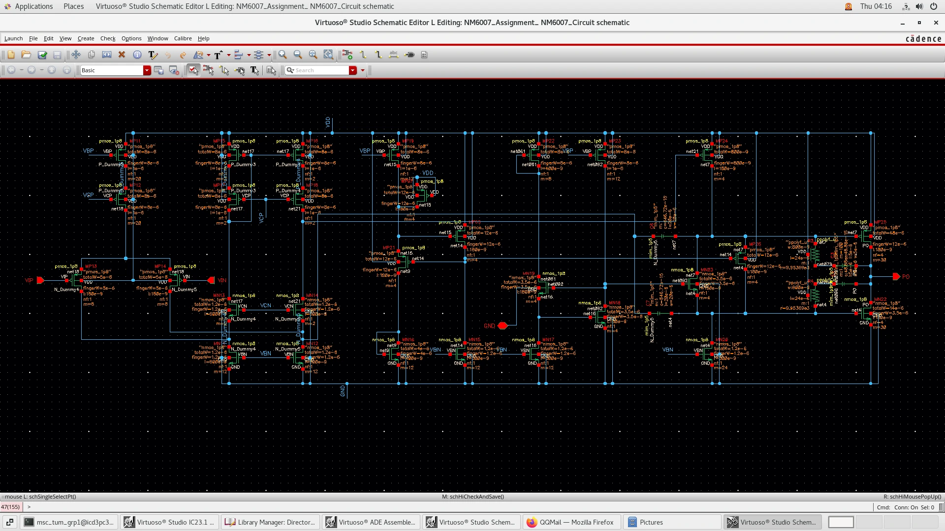
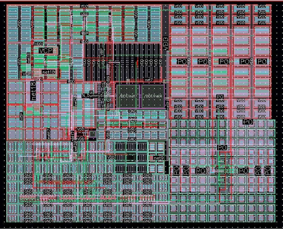
Class-AB Audio Amplifier with Translinear Loop
An independently completed Analog IC Laboratory project in GF 0.18 µm CMOS, covering transistor-level design, full-custom layout, extraction, and post-layout simulation.
Design scope
Bias and start-up circuitry, PMOS/NMOS translinear loops, Class-AB output stage, device-sizing iterations, and Ahuja compensation.
- Process
- GF 0.18 µm CMOS
- Role
- Independent project
- Flow
- Virtuoso schematic → layout → Calibre DRC/LVS/PEX → extracted-view simulation
Simulation results
| Metric | Pre-layout | Post-layout |
|---|---|---|
| Gain | 12.0411 dB | 12.0411 dB |
| UGBW | 305.36 kHz | 305.084 kHz |
| Phase margin | 81.95° | 79.23° |
| THD | −89.86 dB | −83.4 dB |
| Slew rate | 18.6 V/µs | 18.02 V/µs |
| Current | 1.357 mA | 1.201 mA |
Results from my lab report. Each metric uses its own test setup.
PSRR fell short of the ≤−70 dB target: −61.3 dB before layout and −60.056 dB after extraction.
Process corners
The report includes TT/FF/SS/FS/SF process-corner work and documented combinations involving 1.5 V/1.8 V supplies and −40°C/100°C; it is not described as exhaustive PVT sign-off.